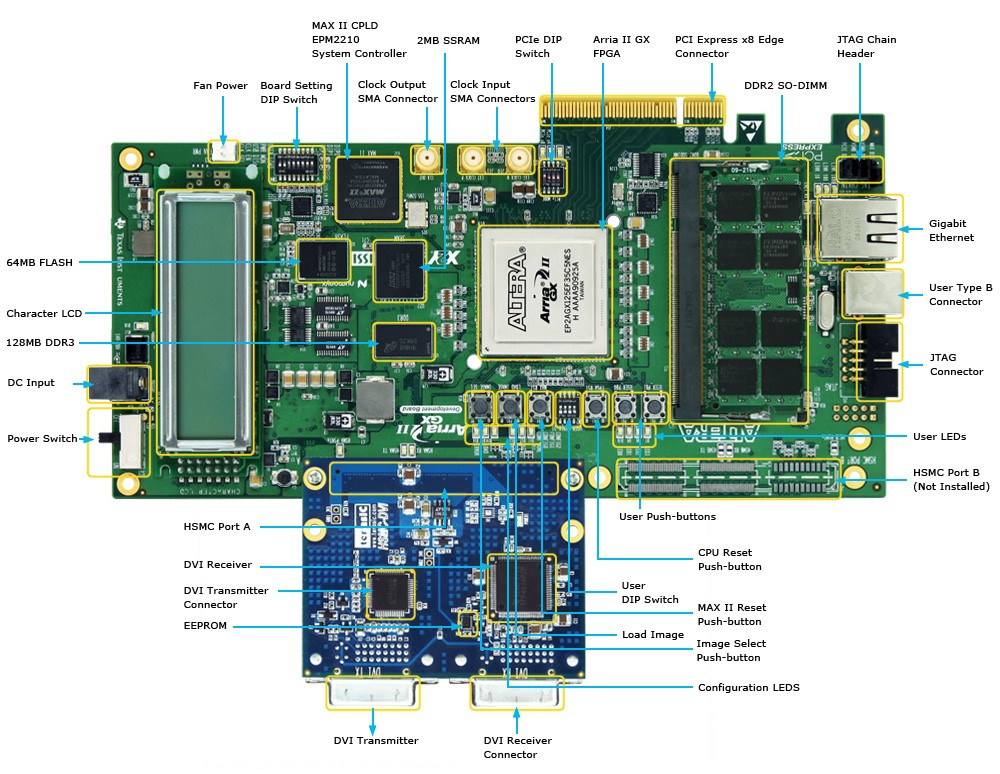
Hello everyone today let us talk about Arria II GX Video Development system which provide high functionality and high connectivity. The Arria II GX Video Development System is an ideal video processing platform for high-end video applications. Terasic recognized for its strong design expertise in high-end video, imaging and multimedia products have made available a video development package that targets video processing development using an Arria II GX device. The package includes an Arria II GX FPGA development kit (DK-DEV-2AGX125N) featuring an EP2AGX FPGA device with HSMC connectors to allow additional functionality and connectivity via HSMC daughter boards. The Arria II GX FPGA development kit delivers a complete PCI Express-based development platform. This interface uses the Arria II GX device’s PCI Express hard IP to accelerate development time for high-volume PCI Express applications including add-in cards, host bus adapters, graphics cards, and high-end servers. Furthermore, the board includes an abundant amount of memory including on-board DDR3 device and DDR2 SODIMM, creating a complete integrated memory interface solution for memory-intensive applications.
The DVI-HSMC daughter card part of the bundled package will allow developers to access high quality and high resolution video signals that can support resolution up to 1600×1200. A complete DVI video controller design with source code is provided.
The development can also allow users to experience advanced image processing designs incorporating VIP (Altera’s Video and Image Processing Suite MegaCore Functions).
Hardware Specification
FPGA Development Kits for Altera Arria® II GX are complete design environments that include both the hardware and software needed to develop Arria II GX FPGA designs. The PCI-SIG-compliant boards and the one-year license for the Quartus® II software provide everything the user needs to begin developing custom Arria II GX FPGA designs.
The Arria II GX-260 FPGA development board is a video development package that targets video processing development using an Arria II GX device. It provides a hardware platform that features sixteen 6.375Gbps transceivers and up to 1.25Gbps LVDS support. With the Arria II GX-260 FPGA, customers can achieve power-reduction benefits while providing high functionality for applications with significantly higher bandwidth requirements.
Arria II GX Development Board:
Arria II GX EP2AGX125EF35 FPGA
- 124,100 logic elements (LEs)
- 49,640 adaptive logic modules (ALMs)
- 8,121 Kb on-chip memory
- 12 high-speed transceivers
- 6 phase-locked loops (PLLs)
- 576 18×18 multipliers
- 0.9V core power
Max® II EPM2210F256 CPLD
- 2.5V core power
On-board ports
- One HSMC expansion port
- One gigabit Ethernet port
PCI Express x8 Edge Connector
- Support connection speed of Gen1 at 2.5Gbps/lane
- Connection established with PC motherboard with x8 PCI Express slot
On-board Memory
- 128MB 16bit DDR3 device
- 1GB 64bit DDR2 SO-DIMM
- 2MB SSRAM
- 64MB FLASH
FPGA Configuration Circuitry
- MAX II CPLD and flash fast passive parallel configuration
- On-board USB-Blaster™ circuitry using the Quartus II Programmer
On-board Clocking Circuitry
- Four on-board oscillators
- 100MHz
- Programmable oscillator, default frequency 125MHz
- Programmable oscillator, default frequency 100MHz
- 155.52MHz
- SMA connectors for external LVPECL clock input
- SMA connector for clock output
General User I/O
- LEDs/displays
- Four user LEDs
- Two-line character LCD display
- One configuration-done LED
- One HSMC interface transmit/receive LED (Tx/Rx)
- Three PCI Express LEDs
- Five Ethernet LEDs
Push-buttons
- One user reset (CPU reset)
- One MAX II CPLD reset
- One load image (program FPGA from flash)
- One image select (select image to load from flash)
- Two general user push-buttons
DIP Switches
- Four user DIP switches
- Eight MAX II device control DIP switches
Power Supply
- 14V to 20V DC input
- PCI Express edge connector power
- On-board power measurement circuitry
Arria II GX FPGA Development Kit CD-ROM
- Design examples
- Board Update Portal, featuring the Nios® II processor web server and remote system update
- Board test system
Altera’s Complete Design Suite DVD
- Quartus II Software Development Kit Edition, includes support for Arria II GX FPGAs
- Nios II Embedded Design Suite
- MegaCore® IP Library includes PCI Express, Triple Speed Ethernet, SDI, and DDR3 High-Performance Controller IP cores
- IP evaluation available through OpenCore Plus
DVI-HSMC Card:
Digital Transmitter
- One DVI transmitter with single transmitting port
- Digital Visual Interface (DVI) Compliant
- Supports resolutions from VGA to UXGA (25 MHz – 165 MHz Pixel Rates)
- Universal Graphics Controller Interface
- 12-Bit, Dual-Edge and 24-Bit, Single-Edge Input Modes
- Adjustable 1.1 V to 1.8 V and Standard 3.3 V CMOS Input Signal Levels
- Fully Differential and Single-Ended Input Clocking Modes
- Standard Intel 12-Bit Digital Video Port Compatible as on Intel™ 81x Chipsets
- Enhanced PLL Noise Immunity
- On-Chip Regulators and Bypass Capacitors for Reducing System Costs
- Enhanced Jitter Performance
- No HSYNC Jitter Anomaly
- Negligible Data-Dependent Jitter
- Programmable Using I²C Serial Interface
- Single 3.3-V Supply Operation
Digital Receiver
- One DVI receiver with single receiving port
- Supports UXGA Resolution (Output Pixel Rates Up to 165 MHz)
- Digital Visual Interface (DVI) Specification Compliant
Altera Arria® II GX and GZ Low Power 6G Transceiver FPGAs deliver substantial cost and power savings over competing devices, while providing high functionality for 6G transceiver-based applications. The 40nm Arria II family includes the lowest cost FPGA with 6.375Gbps transceivers and devices with up to 50 percent lower static power vs. the competition. The Arria II GX FPGAs have up to 16 6.375Gbps transceivers, LVDS at 1.25Gbps, and support for 400MHz DD3. The Arria II GZ FPGA offers up to 24 6.375Gbps transceivers, more density and memory, and higher digital signal processing (DSP) capabilities than Arria II GX FPGAs.
In this abiding endeavor of keeping our customers happy in bringing the new products, Tenet Technetronics is more than happy to set up an Authorized Distribution Alliance with MYIR tech and promote as well as distribute the MYIR tech products in India
Continued with this, there are a lot of activities (Workshops/Videos/Application notes) please stay tuned with our YouTube channel as well as blogs to learn more. (Website: https://www.tenettech.com/browse/FPGA)
For any further assistance, please feel free to contact us at info@tenettech.com and we would be more than happy to help.
Link To buy :
https://www.tenettech.com/product/arria-ii-gx-video-development-system


