System on chip designs improve performance and reduce power consumption as well as semiconductor die area needed for an equivalent design composed of discrete modules, at the cost of reduced replace ability of components.
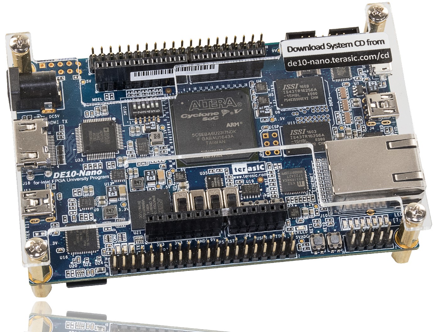
So today let’s start with DE10-Nano development kit which is SOC FPGA
The DE10-Nano development kit featuring a Cyclone® V SOC FPGA, is a robust hardware design platform for makers, educators, and IOT system developers and hardware design platform is built around the Intel System-on-Chip (SOC) FPGA, which combines the latest dual-core Cortex-A9 embedded cores with industry-leading programmable logic for ultimate design flexibility.
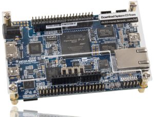
The DE10-Nano development board is equipped with high-speed DDR3 memory, analog-to-digital capabilities, Ethernet networking, and much more that promises many exciting applications.
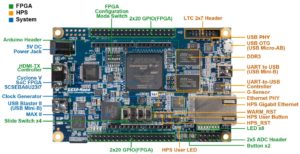
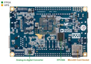
The DE10-Nano board has many features that allow users to implement a wide range of designed circuits, from simple circuits to various multimedia projects.
The following hardware is provided on the board:
FPGA Device
- Intel Cyclone® V SE 5CSEBA6U23I7 device (110K LEs)
- Serial configuration device – EPCS64 (revision B2 or later)
- USB-Blaster II onboard for programming; JTAG Mode
- HDMI TX, compatible with DVI 1.0 and HDCP v1.4
- 2 push-buttons
- 4 slide switches
- 8 green user LEDs
- Three 50MHz clock sources from the clock generator
- Two 40-pin expansion headers
- One Arduino expansion header (Uno R3 compatibility), can be connected with Arduino shields
- One 10-pin Analog input expansion header (shared with Arduino Analog input)
- A/D converter, 4-pin SPI interface with FPGA
HPS (Hard Processor System)
- 800MHz Dual-core ARM Cortex-A9 processor
- 1GB DDR3 SDRAM (32-bit data bus)
- 1 Gigabit Ethernet PHY with RJ45 connector
- USB OTG Port, USB Micro-AB connector
- Micro SD card socket
- Accelerometer (I2C interface + interrupt)
- UART to USB, USB Mini-B connector
- Warm reset button and cold reset button
- One user button and one user LED
- LTC 2×7 expansion header
Block Diagram of the DE10-Nano Board
All the connections are established through the Cyclone V SOC FPGA device to provide maximum flexibility for users. Users can configure the FPGA to implement any system design.
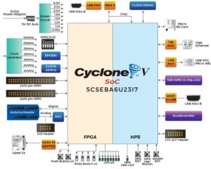
Detailed information about Figure are listed below
FPGA Device
- Cyclone V SoC 5CSEBA6U23I7 Device
- Dual-core ARM Cortex-A9 (HPS)
- 110K programmable logic elements
- 5,570 Kbits embedded memory
- 6 fractional PLLs
Configuration and Debug
- Serial configuration device – EPCS64 on FPGA
- Onboard USB-Blaster II (Mini-B USB connector)
Memory Device
- 1GB (2x256Mx16) DDR3 SDRAM on HPS
- Micro SD card socket on HPS
Communication
- One USB 2.0 OTG (ULPI interface with USB Micro-AB connector)
- UART to USB (USB Mini-B connector)l 10/100/1000 Ethernet
Connectors
- Two 40-pin expansion headers
- Arduino expansion header
- One 10-pin ADC input header
- One LTC connector (one Serial Peripheral Interface (SPI) Master ,one I2C and onel GPIO interface )
Display
- HDMI TX, compatible with DVI v1.0 and HDCP v1.4
ADC
- 12-Bit Resolution, 500Ksps Sampling Rate. SPI Interface
- 8-Channel Analog Input. Input Range : 0V ~ 4.096V
Switches, Buttons, and Indicators
- 3 user Keys (FPGA x2, HPS x1)
- 4 user switches (FPGA x4)
- 9 user LEDs (FPGA x8, HPS x 1)
- 2 HPS reset buttons (HPS RESET and HPS WARM RST )
Sensors
- G-Sensor on HPS
Power
- 5V DC input
We can conclude saying DE10-Nano development kit allows the Users to take the power of tremendous re-configurability paired with a high-performance, low-power processor system.
Continued with this, there are a lot of activities (Workshops/Videos/Application notes) please stay tuned with our YouTube channel as well as blogs to learn more. (Website: https://www.tenettech.com/browse/fpga-6)
For any further assistance, please feel free to contact us at info@tenettech.com and we would be more than happy to help.

